Wednesday, February 24, 2016

Week Seven Blog

Week Seven Blog:

1. Force sensing resistor gives a resistance value with respect to the force that is applied on it. Try different loads (Pinching, squeezing with objects, etc.) and write down the resistance values. 
The resistance value decreases as more pressure is applied to the force sensor. This results in a higher current passing through the circuit.

2.  7 Segment display: 
     
      a) Check the manual of the 7 segment display. Which line lit up? Using package dimensions           and function for B, explain the operation of the display by lighting up different segments. 

          When we connect the resistor to pin 1, segment a lights up; when we connect the resistor to pin           2, segment f lights up. Pin 3 and 14 are the input power sources and pins 4, 5, 6, 9, and 12 are             not used. All the other pins are connected to different segments of the display.

This is a video of us lighting up different segments of the display.

     b) Using resistors for each segment, make the display show 0 and 5.

         To display 0, all of the segments of the display expect segment g is are connected. To display 5,          all of the segments but b and e are connected by resistors. Below are pictures of the 7 segment            display showing 0 and 5.

This is the set up of resistors connected to the 7 segment
display the show the number 0.

This is the set up of resistors connected to the 7 segment 
display the show the number 5.

3.  Display driver (7447):

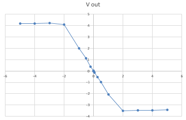
     a) By connecting inputs either 0V or 5V, check the output voltages of the driver. Explain                how the inputs and outputs are related. Provide two different input combinations. 


Photo shows how the 7447 shows 3.


Photo shows how the 7447 shows 6.


Each output corresponds to a different segment of the 7 segment display and will light up a different number depending on the inputs used. Given a certain number inputted in a binary sequence, the corresponding output segments will be displayed as per the table above.


      b) Connect the display driver to the 7 segment display. Verify your question 3a outputs with           those input combinations. 


With the display driver now hooked up to the 7 segment display, we can properly show that the driver does output the right sequence of pins to display the correct numbers that we had discussed in part a. The video below shows the 7 segment display displaying the number we guessed in for the second part of part a.


Video showing the different segments that will light up to display 6. 


4. 555 timer: 
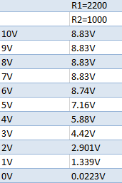
a. Construct the circuit in Fig. 14 of the 555 timer data sheet. Vcc=5V. No Rl. Ra=150k Rb=300k and C=1microF. 0.01 microF capacitor is somewhat larger in size. Observe your output voltage at pin 3 by oscilloscope.


Photo of oscilloscope reading output voltage at pin 3


Photo measuring output voltage at pin 3


b. Does your frequency and duty cycle match with the theoretical value? Explain your work.
Yes, the frequency and duty cycle match with the theoretical values. Our theoretical duty cycle is 0.4. Our theoretical frequency is 1.92. Our measured duty cycle was 0.42 and our measured frequency was 1.98.

c. Connect the force sensing resistor in series with Ra. How can you make the circuit give an output? Can the frequency of the output be modified with the force sensing resistor?  

The circuit will give an output if a big enough force is applied to the force sensing resistor. The frequency of the output will be modified with the force sensing resistor if more or less force is applied.

5. BCD (74192): Connect your 555 timer output to pin 5 of 74192. Observe the input and each output on the oscilloscope.


The input wave has a very high frequency. When the outputs are measured, each one has a different wave configuration. One pin has 2 quick jumps with a break in between, another one has slow low frequency waves. Each pin outputs a different wave pattern. 


6. XOR gate (7486): 
a. By choosing different input combinations, prove the XOR operation through the LED. 
Video showing the different wave configurations

If both pins are connected to the same terminal, they will cancel out and the LED will not light on. The LED lights on when the two inputs are opposite of each other. 

b. Connect the XOR's inputs to the BCD C and D outputs. Explain your observation.
Video showing the C and D configuration

When the inputs are connected to C and D outputs, the LED has a consistent but very slow wave pattern. It would turn on for a couple of seconds, then turn off for a couple of seconds, repeatedly. 

c. Draw the 555 timer, the 74192 A, B, C, and D outputs, and the XOR output. 


7. Connect the entire circuit. Make a video and draw the circuit schematic. 

This is the schematic for the entire circuit displayed
in the video below.

This is a video of the entire circuit running using a 
force sensor to start and stop the counting.

When the circuit is completed, the counting will only happen as the force sensor is pressed. When it is released, the LED will stay in the state that it is in, until it is pressed again.

8. Using other logic gates provided, come up with a different LED lighting scheme. 
Video showing different chip results

Video showing different chip results

Monday, February 15, 2016

Week Six Blog


1.  You will use the OPAMP in "open-loop" configuration in this part, where input signals will be applied directly to the pins 2 and 3. 

a.  Apply 0V to the inverting input. Sweep the non-inverting input (Vin) from -5V to 5V with 1V steps. Take more steps around 0V. Create a table for Vin and Vout. Plot the data. Disuss your results. What would be the ideal plot?
Table of Vin and Vout for non-inverting amplifier

Plot of Vin and Vout for table above

The ideal plot would show Vout ranging from 5V to -5V. Our amplifier was not ideal, so there was some loss of voltage. There was a very high gain because of the open loop, so instead of amplifying the voltage proportionally, it just reaches the maximum and minimum values. 


b.  Repeat part A for the non-inverting input.

Table of Vin and Vout for inverting amplifier

Plot of Vin and Vout for table above

The ideal plot would range from -5V to 5V. This is because of the same reason listed above. This is equal and opposite to the reading above because it is inverted. 


2.  Create a non-inverting amplifier. (R2= 2K, R1=1K). Sweep Vin from -10V to 10V with 1V steps. Create a table for Vin and Vout. Plot the measured and calculated data together.

Table for Vin and Vout of non-inverting amplifier
Plot for Vin and Vout for table above

This is the data gathered from the non-inverting amplifier with R1=1K and R2=2K. It's very similar to the plot we expected to see. Instead of an immediate switch at 0V like the open experiments, there is a linear rise from negative to positive output voltage. 


3.  Repeat part 2 with an inverting amplifier.

Table of Vin and Vout for an inverting amplifier
Plot of Vin and Vout for the table above

These observations are equal and opposite to the values above because it is an inverting amplifier. 


4.  Explain how an OPAMP works. How come the gain of the OPAMP in the open loop configuration is too high but inverting/non-inverting amplifier configurations provide such a small gain?

An OPAMP generates a higher output voltage than what is input. It is used to amplify a signal larger than normal. When the OPAMP is in the open loop configuration, it produces a gain so high that the voltage maxes out at the upper and lower limits long before before it reaches a half of a volt. The inverting/non-inverting amplifier configurations provide a small gain because the resistors keep the difference between the positive and negative inputs smaller.


Temperature Control:

As the heat applied to the temperature sensor increases, the voltage output will increase linearly as well.


Relay:

1.     Connect your DC power supply to pin 2 and ground pin 5. Set your power supply to 0V. Switch your multimeter to measure the resistance mode; use your multimeter to measure the resistance between pin 4 and pin 1. Do the same measurement between pin 3 and pin 1. Explain your finding.

The resistance value between pin 4 and pin 1 was 0Ω. The resistance value between pin 3 and pin 1 was 200Ω.


2.   Now sweep your DC power supply from 0V to 8V and back to 0V. What do you observe at the multimeter? Did you hear a clicking sound? How many times? What is the threshold voltage value that cause the switching?
 
When we hear the relay make a clicking sound, we know that it has "switched" between pin 3 and pin 4. The threshold voltage value to change pins is 6V when we increased the voltage. When decreasing, the lower threshold voltage value was around 2.5V. These are the points at which you hear the clicking sound.


3.     How does the relay work? Apply a seperate DC voltage of 5V to pin 1. Check the voltage value of pin 3 and pin 4 while switching the relay.

When reading the voltage values at pin 3 and 4, we noticed that while one pin has a readable voltage value, the other pin reads 0V. After reaching the threshold voltage value, allowing the relay to switch, the pin that originally had a readable value now reads 0V and the pin that read 0V orginally now reads the value that the other pin originally read.


LED + Relay


This video shows the relay switching. When the voltage is increased, there is a clicking sound and the LED lights on. This shows that the threshold voltage value has been reached. The voltage is decreased and the LED shuts off when the lower threshold value is reached.      


Operational Amplifier:

1.  Connect the power supplies to the op-amp. Show the operation of LM 124 operational amplifier in DC mode with a non-inverting amplifier configuration. Choose any opamp in the IC.
Table for R1=1000 and R2=2200

Table for R1=2200 and R2=1000


Table for R1=1000 and R2=12000


Table for R1=1000 and R2=3000


Table for R1=2200 and R2-3000


As you can see in all 5 of these experiments, all of them have a very similar maximum voltage value. This tells us that the upper limit of the amplifier is unaffected by the resistor configuration. The only difference between the graphs is the rate at which the output voltage drops to zero as in the input voltage goes to zero.

2.     Use your temperature sensor as your input. Do you think you can generate enough voltage to trigger the relay.

No, we can not generate enough voltage with this set up. We need roughly 6V to trigger the relay. The temperature sensor would output only around 1.6-1.7V. To get this to 6V, we would need almost 400 degrees Celsius, which would most definitely melt the breadboard.

3.    We added a non-inverting amplifier to the V out of the temperature sensor to increase it's signal large enough to turn on the LED.


4.


Sunday, February 14, 2016

Week Five Blog


1. Perform the functional check. 

A functional check should be done before using an Oscilloscope the first time, or the first time after a long time. A functional check will test whether the oscilloscope is working correctly or not.
This is the displayed wave after the functional check.


2. Perform manual probe compensation.

Manual probe compensation is where you manually adjust the probe to fine tune it with the oscilloscope. If the probe is not compensated, the probe could be under compensated or over compensated which will make the probe measurements wrong. Below is a picture of our probes before the manual probe compensation. As you can see the wave peaks are not flat, this means the probes were over compensated to begin with. The second picture is displaying the readings after the adjustment, as you can see the wave peaks are flat which means the probes are compensated correctly.

This is the wave when the probe is over compensated.


This is the wave when the probe is corrected.


3. What does probe attenuation (1x vs 10x) do?
 
Probe attenuation allows the user to control the bandwidth on the oscilloscope. The 10x setting allows you to use the full bandwidth while the 1x setting limits the oscilloscope bandwidth to 7 MHz.


4. How do vertical and horizontal controls work? Why would you need it?
   
The vertical control allows you to shift the wave up or down with respect to the center axis. The horizontal control allows you to shift the wave left or right with respect to the center axis. These functions are helpful when you want to read more than one waveform at a time and want to place them over each other or above and below each other for comparison.


5. Generate a 1 kHz, 1 Vpp around a DC 2V from the function generator.
   
    a. Connect this to the oscilloscope and verify the input signal using the horizontal and vertical readings.
   
Each horizontal line is separated vertically by 0.5 volts. Our signal reached from the origin to one line above and one line below. This means that from the origin, the wave reaches +0.5V and -0.5V. 0.5-(-0.5)=1 V peak to peak.


This is wave from the setup above, centered on the origin.

      b. Figure out how to measure the signal properties using menu buttons on the scope.
   
When trying to measure signal properties, you should press measure, then source CH 1, then you can cycle through the properties by pressing type. 


6.  Connect function generator and oscilloscope probes switched. What happens? Why?

When switching the probes, we noticed that the oscilloscope couldn't come up with a distinct measurement. The value is basically zero and noise is displayed. This is because the gator clip on the oscilloscope probe is connected to ground on the oscilloscope. So if you switch them, you are grounding the signal before the probe can read it.
?


7.  After calibrating the second probe, implement the voltage divider current below. Measure the following voltages using the Oscilloscope and comment on your results:


a. Va and Vb at the same time.

       
The Va and Vb voltages from the problem above.
      The peak to peak voltage of Vb, which is the top wave, is 496mV which means the wave has an amplitude of 248mV. The peak to peak voltage of Va, which is the second value, is 264mV which means the wave has an amplitude of 132mV.


      b. Voltage across R4.

      In the picture below is the same circuit and probe connections as in part a, but this time the red wave line is the measured difference between Vb and Va. This is helpful because it is the voltage drop over the R4 resistor, which is the same thing as the voltage across R4.

The same circuit and probe connects as part a, but now with
a measured difference wave.

8. For the same circuit above, measure Va and Vb using the handheld DMM both in AC and DC mode. What are your findings? Explain.

The table below are the measurements of Va, Vb, and R4 using a handheld DMM to measure both AC and DC voltages. We found that the AC voltages measured matched the RMS voltages from the previous experiment. We also found that the difference between Vb and Va matched with the measured value for R4.


9. For the circuit below:


     a. Calculate R so the given voltage values are satisfied and make a video explaining.

         The video below gives a detailed explanation of how to calculate R so the given voltages are satisfied. The calculated R value is 2.5k ohm.


     b. Construct the circuit and measure the values with the DMM and oscilloscope.

      This video shows the circuit constructed and the wave generated
      although the numbers don't match part a above. This is because 
      the voltage input values are different.


10. Operational amplifier basics: Construct the following circuits using the pin diagram of the opamp. The half circle on top of the pin diagram corresponds to the notch on the integrated circuit (IC). Explanations of the pin numbers are below:


a. Inverting Amplifier: Rin = 1k, Rf = 5k. Apply 1 Vpp @ 1kHz. Observe input and     output at the same time. What happens if you slowly increase the input voltage up     to 5V? Explain your findings.

      When the input voltage increases from 0.5V to 5.0V, the peak to peak value of the wave will increase until it reaches 10V, there the value will no longer increase even if the input voltage keeps increasing. In this video the Vout reached 10Vpp at around Vin = 1V, from there the output voltage no longer increased, even when we got to Vin = 5V, Vout still only read 10Vpp.


      b. Non-inverting Amplifier: R1 = 1k, Rf = 5k. Apply 1 Vpp @ 1kHz. Observe input and output at the same time. What happens if you slowly increase the input       voltage up to 5V? Explain your findings.

The voltage out on the non-inverted amplifier starts relatively close to the voltage in when the voltage in is small. But as the voltage in increases, the voltage out increases far greater. But just like the inverted amplifier, this amplifier stops increasing after a certain voltage value. The voltage out for this amplifier stops at Vout = 20Vpp. The video below shows this happening.


Wednesday, February 3, 2016

Week Four Blog

Week Four Blog:

1. Use the transistor by itself. The goal is to create the graph for IC versus VBE. Connect base and collector. Use 10k potentiometer to generate the voltage. Use 5V but DO NOT EXCEED 1V for VBE. Make sure you have the required voltage value set before applying it to the base. Transistor might get really hot. Do not TOUCH THE TRANSISTOR! Make sure to get enough data points to graph.
Table of the data points collected at
IC and VBE.
Graph of  the data point in the table to the right.


2. Create the graph for IC versus VCE. Vary VCE from 0V to 5V. Do this measurement for 3 different VBE values: 0V, 0.7V, and 0.8V. The circuit should look like:


Circuit Design.


Graph of the measured current over the collector versus
the voltage difference of the collector to the emitter,
for a given voltage difference over the base to the emitter.


3. Apply the following bias voltages and fill out the table. How is IC and IB related? Does your data support your theory?

Table of voltage and current values of
a transistor.
As the voltage being applied to the base of the transistor increases both the current of the collector and the current of the base. But the current of the collector increases at a significantly higher interval than the current of the base. This data supports the theories of VBE vs IC and VBE vs IB that states that IC will increases exponentially and IB will increase but at a near zero rate.


4. Explain photocell outputs with different light settings. Create a table for the light conditions and photocell resistance.

A photocell works by changing its resistance values based on the amount of light that reaches the cell. The more light it receives the smaller the resistance value is; likewise the less light it receives the higher the resistance values becomes.

Table of resistance values of
the photocell at varying light levels


5. Apply voltage (0 to 5V with 1V steps) to DC motor directly and measure the current using the DMM.


Table of the currents measured
in the DC motor at given voltages


6. Apply 2V to the DC motor and measure the current. Repeat this by increasing the load on the DC motor. Slighting pinching the shaft would do the trick.


As the load on the DC motor is increased the current measured across the motor also increases. Below is a table showing the change in the current across the table when the load on the motor is increased.

Table showing the change in current
when load is increased on the DC motor


7. Create the circuit below. Explain the operation in detail.


Circuit design of the DC motor that
incorporates a photoresistor.


In this circuit a 5V power source goes through a photoresistor and splits between the base pin of a transistor and a 1k resistor. The voltage going to the base of the transistor activates the transistor allowing the current and voltage of the other power source to flow through. From the 10V power source the voltage travels through a 47 Ohm resistor into the collector of the transistor. If there is enough voltage being applied to the base, the voltage continues through the transistor into the DC motor which causes the motor to spin. If the resistance value of the photoresistor is too great, not enough voltage will reach the base of the transistor and the DC motor will not activate.

Below is the video of the above circuit in application.


8. Explain R4's role by changing its value to a smaller and bigger resistors and observing the voltage and current at the collector of the transistor.


The resistor R4 buffers the transistor from the voltage being inputted by the power source. If we decrease the resistance value in R4 the current and voltage at the collector of the transistor will increase. Likewise, if the resistance value for R4 is increased then the current and voltage across the collector become smaller.

9. Create your own Rube Goldberg setup.

Our Rube Goldberg design is to use the DC motor to wind up a piece of floss, shortening it so that it flips a bowl over to deposit food into Matt's fish bowl. Henry the VIII, Matt's fish, demands that Matt feeds him the moment he turns on the light when he comes home.

In the video we show how the design works in application. We could not shut the room lights off in the video because there were other people in the lab that needed the lights on. We simulated having the room lights off by Matt putting his finger over the photoresistor. In the video you can hear the power source being switched on but nothing happens until Matt removes his hand from the photocell. This way, the circuit can be switched on when Matt leaves for the day but Henry the VIII will only be fed when Matt returns and turns on the lights.


This is the video of our Rube Goldberg Design in application.